Why Is Debonding Important in Advanced Manufacturing Processes?
2026-04-07
What is debonding? Why is TBDB so important in advanced manufacturing processes? This article explains the definitions, processes, and typical temporary bonding and debonding technologies, while also introducing how debonding is applied in the semiconductor industry. If you are looking for debonding materials for advanced manufacturing processes, SEKISUI Chemical is ready to help.
What Is Debonding? An Introduction to Four Major Debonding Technologies
Technologies such as temporary bonding and debonding are widely used in the industry to prevent wafer damage during processing in the wafer manufacturing process and solve related issues. Here, we explain the definitions and processes of temporary bonding and debonding in detail and introduce the principles, advantages, and disadvantages of four typical debonding technologies.
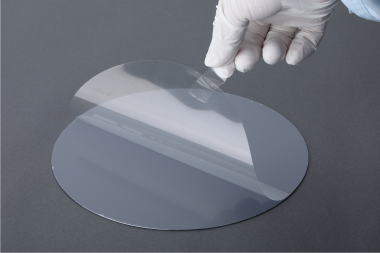
(1) What Is Temporary Bonding? What Is Debonding (Release)?
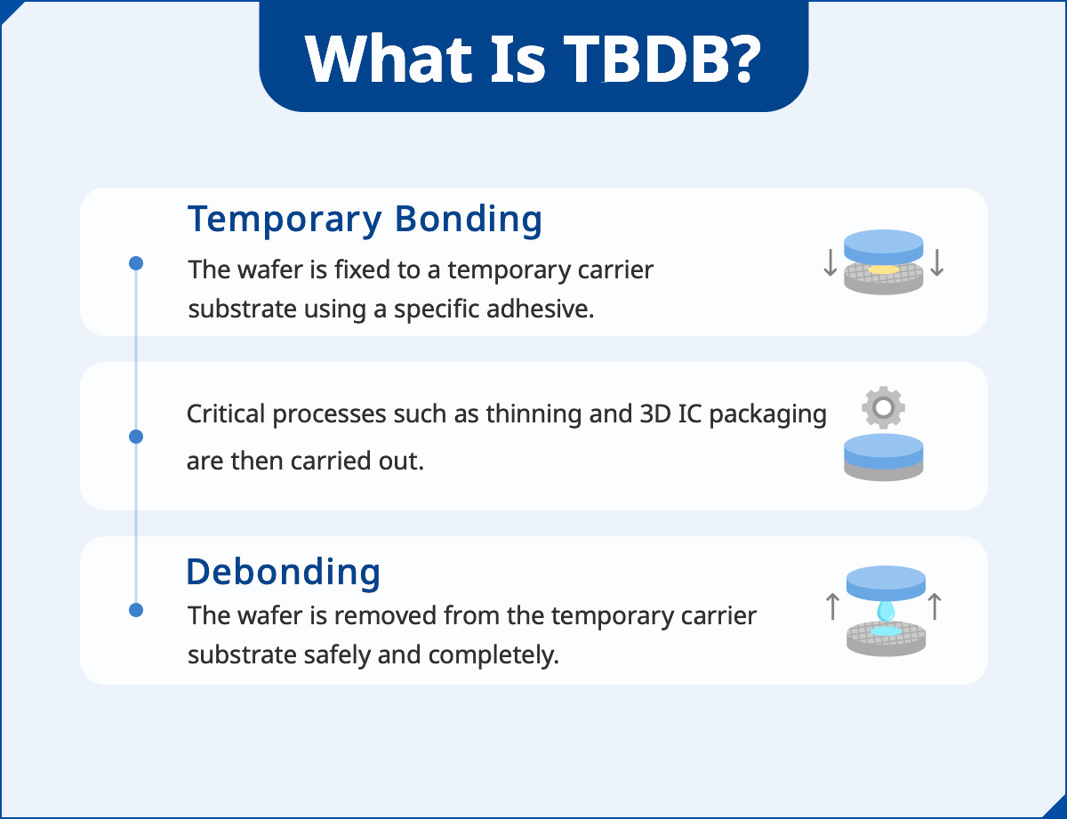
In advanced semiconductor manufacturing processes, wafers go through complex steps such as polishing, thinning, and 3D IC packaging to become chips with the appropriate size and sufficient performance. However, because each step involves highly precise treatment of the wafer, there is a constant risk of damage. For this reason, the wafer is first fixed to a "temporary carrier substrate" with a specific adhesive prior to processing to reduce the incidence of unexpected defects and damage. This process is called temporary bonding.
After the critical manufacturing process is completed, the wafer must then be removed safely and intact. This step of "removing the temporary carrier substrate" is called debonding (release). Because wafers are extremely fragile, and because any adhesive that is not completely removed can affect yield, debonding is an extremely important technology. To move on to subsequent packaging and inspection procedures, the wafer must be fully released without damage.
These two closely connected steps - temporary bonding and debonding - are collectively referred to in the semiconductor industry as "TBDB," and they are indispensable steps in wafer processing.
(2) Explanation and Comparison of Four Major Debonding Technologies
The following are some of the main debonding technologies commonly used in the industry today. Each method requires the combined use of specific tapes or adhesives and has its own advantages and limitations.
1. Laser Lift-Off (LLO) (Laser Debonding)
When removing tape designed for laser debonding, simply directing UV laser energy precisely at the surface generates gas between the tape and the adherend, instantly decomposing the adhesive layer. This debonding technology is well-suited for ultra-thin wafers and offers fast processing with low stress. Although equipment costs are relatively high, it is often the first choice for many precision manufacturing processes.
2. Thermal Debonding
Like laser debonding, thermal debonding also uses specific tapes or adhesives. These maintain adhesion at room temperature, but during debonding, heating softens or decomposes the adhesive and rapidly reduces its adhesion, allowing the wafer and carrier substrate to separate easily. While this technology is relatively simple, a drawback is that the adherend must be thermal resistant. There is also some risk of heat damage to the wafer and carrier substrate.
3. Mechanical Debonding
As the name suggests, mechanical debonding uses general physical methods to separate the wafer from the carrier substrate, and it is often used in mass-production processes. Its advantage is high processing speed, but insufficient control can cause excessive stress, making the wafer prone to breakage.
4. Chemical Debonding
Chemical debonding uses solvents or chemical solutions to dissolve the adhesive, which offers excellent wafer protection. However, it requires additional cleaning and waste liquid treatment, increasing environmental and cost-related burdens. In addition, substances contained in the tape may dissolve out during processing. To avoid this, it is necessary to specially select tapes with exceptional chemical resistance, but such products tend to be limited in choice and higher in cost.
| Debonding Technology | Advantages | Disadvantages |
|---|---|---|
| Laser Lift-Off (LLO) | Fast Low stress Well-suited for ultra-thin wafers |
High equipment cost |
| Thermal Debonding | Simple technology | Material must be thermal resistant Risk of damage to the wafer and carrier substrate |
| Mechanical Debonding | Fast Well-suited e for mass-production processes |
High stress, which can make the wafer prone to breakage |
| Chemical Debonding | Excellent wafer protection | Additional cleaning and waste-liquid treatment required Limited choices of chemically resistant dicing tape, with high cost |
For advanced wafer processing, laser lift-off (LLO) is the optimal solution.
Please contact SEKISUI Chemical for any other support related to debonding.
Examples of Debonding Applications for Semiconductors: Advanced Packaging, Heterogeneous Integration, and Mass Transfer
In semiconductor manufacturing processes, debonding technology can be broadly applied across multiple important stages, including packaging, stacking, and optoelectronic transfer. Here, we explain how debonding technology supports the development of advanced manufacturing processes through three typical applications - advanced packaging, heterogeneous integration, and mass transfer.
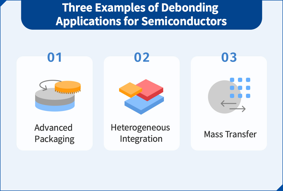
(1) Advanced Packaging
In advanced packaging technology, fan-out, 2.5D packaging, and 3D packaging are among the most difficult manufacturing processes. To improve chip performance and density within limited space, wafers must be thinned to the extreme so that subsequent stacking and redistribution can be carried out. However, once thinned, wafers are extremely fragile, so even a slight mishandling can cause warpage, cracking, or edge chipping.
For this reason, the industry generally uses TBDB technology to stably support wafers even during manufacturing processes that apply high stress, such as polishing, etching, and wiring. After the relevant processes are complete, the wafer is safely separated from the carrier substrate, preventing damage caused by mechanical stress and differences in thermal expansion, enabling high-yield and highly reliable packaging.
(2) Heterogeneous Integration
Heterogeneous integration refers to integrating chips with different functions, processes, and materials - such as logic ICs, memory, sensor elements, optoelectronic devices, or RF modules - vertically or horizontally within the same package system. This technology enables major improvements in system performance and miniaturization without relying solely on the further scaling of a single chip.
However, due to large discrepancies in chip thickness, coefficients of thermal expansion, and material features, problems such as stress deformation, misalignment, and structural warpage are more likely to occur during stacking and bonding if proper support is not provided. Therefore, support from TBDB technology is also necessary to reliably assist the device integration process.
(3) Mass Transfer
In the Micro LED and optoelectronic device manufacturing industries, it is often necessary to transfer tens of thousands of micrometer-scale chips from a wafer to a drive circuit substrate. Because the crystals are extremely small and arranged in high density, even slight misalignment or damage can cause display defects. Consequently, the demands on manufacturing process stability and precision are extremely strict.
Temporarily bonding the wafer to a carrier substrate provides sufficient mechanical strength and flatness so that structural integrity can be maintained during processes such as etching, laser lift-off (LLO), and micro transfer printing. After completion of fine-structure processing, transfer and debonding are carried out. This method not only effectively improves yield, but also ensures precision in dense arrangements, making it a key technology for driving the next generation of display technology.
For these reasons, temporary bonding and debonding technologies are indispensable elements in advanced manufacturing processes. These technologies not only make it possible to achieve both stability and precision in wafer processing procedures, reduce loss, and improve yield, but also support emerging technologies such as heterogeneous integration and optoelectronic transfer. As demand continues to rise for finer processes and chip stacking, the importance of these technologies will only continue to grow.
/SELFA.png)