A Complete Guide to Semiconductor Manufacturing Processes and Principles
2026-04-07
What steps are involved in the semiconductor manufacturing process? How are the chips that are essential to modern electronic devices made? To understand the secrets of semiconductors, we first need to start with what semiconductors are and the principles behind them. This article presents the sequence of the semiconductor manufacturing process, the industry chain, and key packaging materials, and also answers common questions.
What is a Semiconductor? The Materials Behind the Ubiquitous Semiconductor
Semiconductors are the foundation of modern technology. Although they cannot be seen or touched, they quietly support virtually every smart application in daily life. From smartphones and computers to automobiles and medical equipment, the operation of nearly all electronic products depends on semiconductors. To understand this important technology, we must begin with its definition, principles, and material features. So, let us unravel the secrets of the material that changed the world.
(1) What is a semiconductor? How is it different from a wafer, a chip, or a semiconductor device?
A semiconductor is called a “semi-”conductor because its electrical conductivity lies between that of a conductor and an insulator, allowing it to control the passage of electric current under specific conditions. Precisely because of this feature, this type of material is used to manufacture structures involving complex changes in conductivity, enabling the transmission and processing of complex signals and commands, making it a core component of modern electronic products. However, semiconductor materials cannot be used as they are; they become usable only after undergoing a series of processing procedures. The following are products created from semiconductor materials through various kinds of processing.
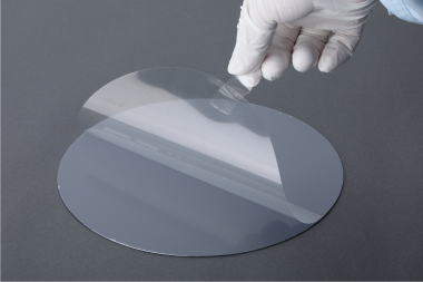
- Wafer: A disk-shaped plate formed by slicing and polishing semiconductor material, used as the substrate in subsequent manufacturing stages.
- Chip: A single small piece cut from a wafer that, after circuit design and packaging, becomes a processor or memory device for practical use.
- Semiconductor device/component: An application device such as a diode, transistor, or integrated circuit manufactured using chip functions.
The relationship among these products can be simplified as: semiconductor material → wafer → chip → semiconductor device.
Chips and semiconductor devices have an extremely wide range of applications. From smartphones, computers, and home appliances to automobiles, medical devices, and communications networks, all are driven and controlled by semiconductors.
(2) Semiconductor materials: the key to enabling the property of “semi-conduction”
So, why are semiconductors able to exhibit this unique semi-conductive behavior? Their special properties come from the fact that the material structure itself has an appropriately sized “band gap.” A band gap refers to the separation between the valence band, the energy band filled with electrons in a solid, and the conduction band, the energy band in which electrons can move freely and conduct electricity. The smaller the band gap, the higher the conductivity. Semiconductors typically have a band gap of about 1 to 3 eV. (Conductors have a band gap of nearly 0, while insulators usually have a band gap of 9 eV or more.) When heated, exposed to light, or stimulated by an electric field, electrons can cross the band gap and move into the conduction band, allowing semiconductors to exhibit semi-conductive behavior.
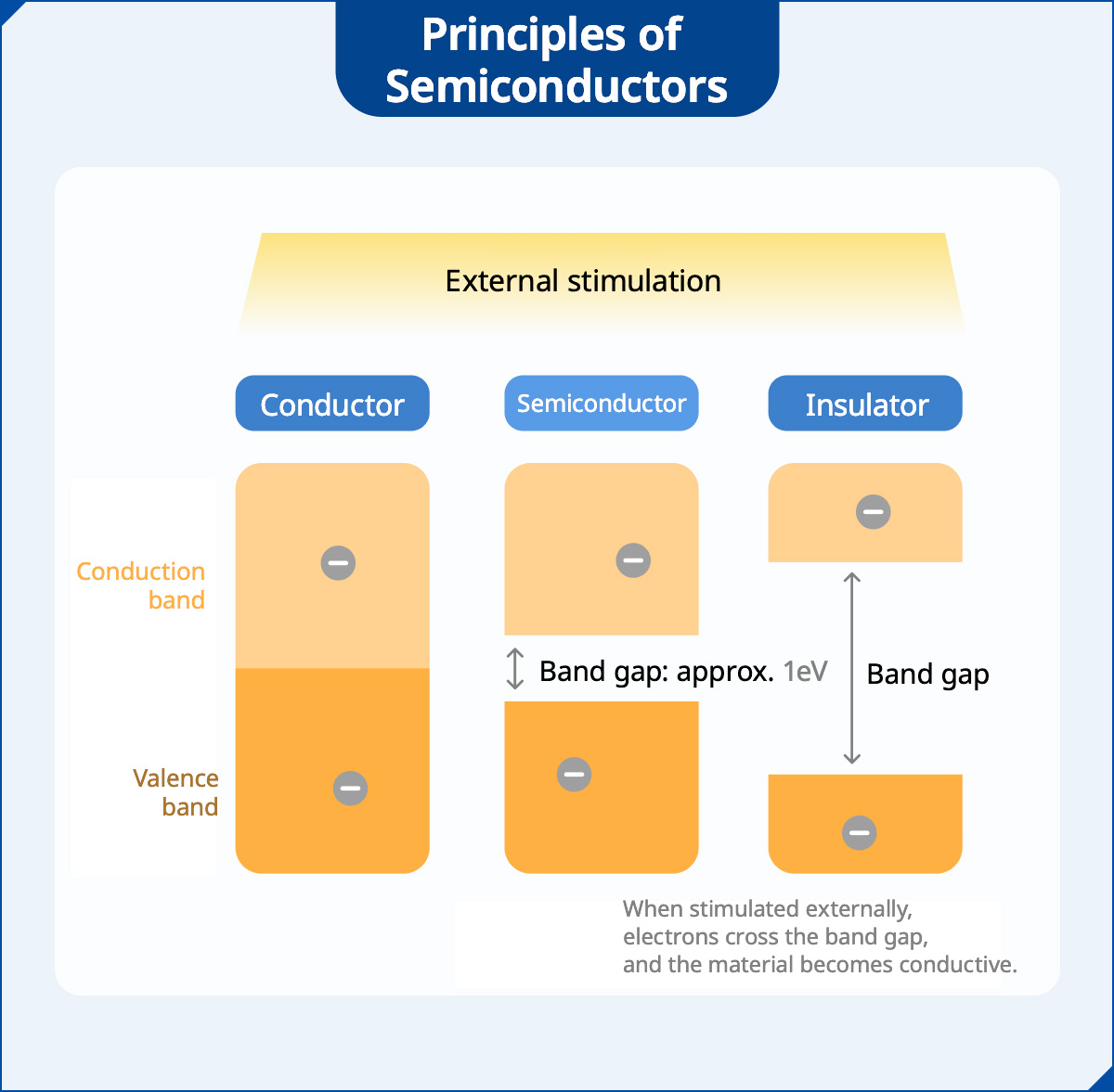
Silicon is the most widely used semiconductor material because it is abundant in nature and its processing technology is now well established. In addition, semiconductors made from materials like germanium (Ge), gallium arsenide (GaAs), and gallium nitride (GaN) demonstrate superior performance in applications such as high frequency, high power, and optoelectronics.
It is also worth noting that, in addition to methods such as heating and light exposure that excite electrons into the conduction band, conductivity can now also be modified through doping. For example, pure silicon itself does not have particularly high conductivity, but by adding elements such as phosphorus or boron, electrons or holes can be adjusted to form n-type or p-type semiconductors. This not only enables the effect of partial conductivity, but also allows precise control of current flow, making it the most widely used technology in modern electronic devices.
- N-type semiconductor: A silicon crystal is doped with a pentavalent element (such as phosphorus or arsenic). These atoms have five valence electrons, so when they bond with silicon, which has four valence electrons, one free electron remains that does not bond. Because this extra electron can move freely through the crystal, conductivity increases.
- P-type semiconductor: In contrast to n-type semiconductors, when a silicon crystal is doped with a trivalent element such as boron (B) or aluminum (Al), each atom has only three valence electrons, so one electron is missing when it bonds with silicon, creating an electron vacancy called a “hole.” Because holes attract nearby electrons to fill the vacancy, their position effectively moves in the direction opposite to the electric field, producing conductive behavior.
Uncovering the Full Picture of Semiconductor Device Manufacturing: Understanding the Eight Steps of Semiconductor Manufacturing and the Industry Chain
You are probably wondering how such mysterious semiconductors are actually manufactured. From here, we provide a comprehensive introduction to the operating model of the semiconductor industry chain and explain the eight major steps of wafer manufacturing. Let us look at how a silicon wafer is endowed with intelligence inside a clean room and ultimately transformed into the heart that powers technology. Through the following detailed explanations and illustrations, you will gain a clearer understanding of the manufacturing process from concept to finished semiconductor product.
(1) From idea to component: an introduction to the semiconductor industry chain
From structural design to actual manufacturing, and from materials to devices, only by investing substantial human resources and materials at every stage can small yet high-performance semiconductor chips be produced, after which they are used by manufacturers across a wide range of fields. The semiconductor industry chain as a whole can be broadly divided into three parts.
- Upstream (design and materials): IC design companies are responsible for circuit architecture design, while material manufacturers supply silicon wafers, photomasks, and chemicals to provide the foundation required for manufacturing.
- Midstream (manufacturing): Foundries precisely convert circuit designs into chips through complex processes such as photolithography, film deposition, and etching.
- Downstream (packaging and testing): After chips are completed, they undergo protective packaging and electrical testing to ensure performance and quality before being shipped to system and brand manufacturers.
After passing through the entire industry chain, chips are configured into various semiconductor devices according to their area of usage and application, and are widely used in smartphones, automobiles, home appliances, medical devices, and many other products, supporting every aspect of modern life.
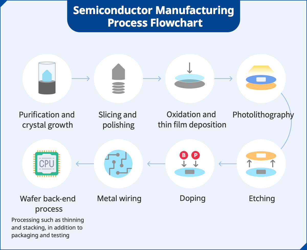
(2) A complete guide to the wafer manufacturing process: deepen your understanding of the sequence and principles of the semiconductor manufacturing process
1. Purification and crystal growth
Natural quartz sand is chemically processed and converted into high-purity polycrystalline silicon, which is then heated and melted. A single-crystal seed is brought into contact with the melt, and a single-crystal silicon ingot is produced using the crystal pulling technique known as the Czochralski (CZ) method, in which the crystal is uniformly pulled. High purity and excellent crystallinity are essential to ensuring chip performance, and even trace impurities can cause defects in back-end processes. For this reason, it is imperative that this stage is handled by highly specialized manufacturers using professional equipment under controlled conditions. It is usually carried out by material manufacturers and serves as the starting point of the wafer manufacturing process.
2. Slicing and polishing
The single-crystal silicon ingot is sliced into thin wafers and, after precision polishing and cleaning, becomes a “bare wafer”. A bare wafer is like a clean, flat blank sheet on which circuit patterns can be formed during back-end processes. If the surface is not sufficiently smooth, subsequent photolithography and etching cannot be carried out accurately.
3. Oxidation and thin film deposition
Next comes the full-scale wafer processing stage. First, an extremely thin silicon dioxide film is formed on the surface of the silicon wafer. This process is called oxidation. The oxide layer serves as insulation and protection, preventing the silicon crystal from coming into contact with conductive metals added in subsequent stages, thereby preventing electrical interference and the diffusion of impurities. After this process, thin film deposition technology is used to coat the wafer surface with multiple functional thin films, such as conductive metal layers and dielectric layers. These structures serve as base materials for later photolithography and etching, forming the foundation for the electrical structural properties of each element within the chip.
4. Photolithography
In photolithography, photoresist coating, exposure, and development are used to transfer circuit design patterns onto the wafer by shining light on it, much like developing a photograph. The narrower the line width, the greater the number of transistors that can be fabricated into a chip, and the higher the computing performance, making this one of the most important steps.
5. Etching
Etching is the step in which unwanted portions after photolithography are removed using chemical solutions or plasma etching, leaving only the required wiring and structures. In this stage, the circuit is finally physically engraved onto the wafer surface, and the basic form of the transistor gradually takes shape. After etching is completed, the photoresist is stripped so that it does not affect back-end processes. Finally, the wafer is cleaned to completely remove residual photoresist fragments and etching by-products, keeping the surface clean so the next step can proceed smoothly.
6. Doping
Trace elements (such as boron and phosphorus) are introduced into the wafer to adjust the conductivity in specific areas and form p-type and n-type semiconductors. This enables transistors to act like switches and allows current flow to be controlled and fine-tuned.
7. Metal wiring
Metal interconnects are arranged on the wafer surface to connect countless transistors, forming a complete circuit network. Like a city’s road network, metal wiring transmits signals at high speed and ultimately ensures the proper operation of the finished chip.
To complete a wafer covered with circuit patterns, it is not unusual to repeat wafer processing steps dozens, and in some cases more than a hundred, times.
8. Wafer back-end processes
The main purpose of the wafer back-end process is to make the wafer thinner and lighter, improve conductivity, and prepare it for subsequent packaging. In this step, thinning, through-hole processing and heterogeneous integration through backside grinding and polishing are first carried out. To maintain stability during processing, temporary bonding and debonding technologies are used to fix the wafer to a carrier substrate during processing and then to release it after completion. Once these processes are finished, the wafer is diced into individual chips for use in the next stage.
Finally, the diced chips move on to the packaging and testing stage. The purpose of packaging is to protect the chips from damage caused by external force, moisture, static electricity, and contamination, while also establishing electrical connections and efficient heat dissipation paths so the chips can operate stably with high efficiency in actual use. Packaging materials play an important role here; they not only protect the chips and enhance heat dissipation, but also establish stable connections between the chips and the circuit board, ensuring stable operation over extended periods of actual use. Finally, electrical and functional tests are conducted to check performance and reliability and to screen out defective products.
After going through this series of back-end processes, the semiconductor device is finally complete and ready for use in various electronic products.
(3) An easy-to-understand flowchart of each step in the semiconductor manufacturing process
After reading through the complex and highly precise manufacturing process described above, you probably now understand the difficulty of the semiconductor manufacturing process. In every respect, from material purity to environmental control and load control, even the slightest mistake can have a serious impact on yield. Even greater care is required in packaging, the final gateway of the manufacturing process, so that the costs invested up to that point are not wasted just prior to the completion of the product.
High-quality packaging materials are indispensable for achieving more precise semiconductor packaging processes. For example, tapes with strong adhesion, easy release, and no adhesive residue, release liners that protect chip surfaces from damage, and particle fillers that ensure electrical and thermal conductivity can all support process progress from different angles and further improve the performance of the finished product.
Why Is the Semiconductor Manufacturing Process So Complex? Answers to Frequently Asked Questions About the Semiconductor Manufacturing Process
Do you still have questions about the semiconductor manufacturing process? Here we summarize and explain three common questions in order: the complexity of the manufacturing steps, the role of packaging materials, and the importance of the packaging and testing stages.
Q1: Why does the semiconductor manufacturing process require so many steps?
The semiconductor manufacturing process is an extremely precise engineering undertaking because it must integrate billions of transistors and complex circuit structures onto a single wafer measuring only a few dozen millimeters. From refining silicon raw materials to photolithography, etching, doping, metal wiring, packaging, and testing, every step must be completed in a clean room with nanometer-level precision in order to ensure performance and yield.
Q2: What roles do semiconductor packaging materials play?
Packaging materials serve both as a protective layer and bridge between the chip and the external world, while simultaneously fulfilling three main functions: mechanical protection, thermal conduction and heat dissipation, and electrical connection. Taking SEKISUI Chemical’s various packaging materials as examples, release liners protect and cushion chip surfaces, metal-plated microparticles are used to adjust electrical and thermal conductivity, and build-up films serve as insulating material between substrates and packaging layers, thereby reducing packaging-related losses.
Q3: Why are packaging and testing so important?
Packaging and testing are the final stages of the semiconductor manufacturing process and determine whether a product can be brought to market. Packaging not only protects chips from external contamination and mechanical damage, but also carries electrical signals accurately to external circuits, so poor design can lead to problems such as insufficient heat dissipation and electrical instability.
During the testing stage, each chip’s functionality, frequency, power consumption, and stability are inspected to check compliance with design specifications and market standards. Only chips that pass rigorous testing are incorporated into electronic products and ultimately become marketable semiconductor devices.
/SELFA.png)
_熱硬化型層間絶縁フィルム_png_w500px_h333px.png)
_ミクロパール™_png_w500px_h333px.png)
_熱プレス工程用離型フィルム_png_w500px_h500px.png)