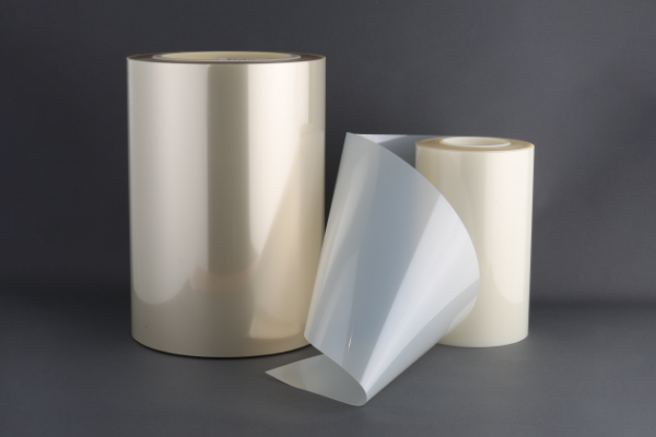
SELFA
“SELFA™” , enabling new semiconductor process by highthermal resistance and debonding technology.
What is SELFA™?
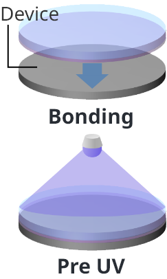
SELFA™ is a UV release tape that achieves strong adhesion and easy peeling. By UV irradiation, N2 gas is generated between the tape and the subject, nullifying adhesion strength and allowing it to be easily peeled off.
It can be easily peeled off without causing any damage to thinly polished wafers.
When is SELFA™ used?
SELFA™ is mainly used in the manufacturing of semiconductor wafers and chips. Currently, we offer a lineup of three types of products for various processes such as package manufacturing, wafer support, and plating processes.
Both single-sided and double-sided types are available based on different applications.
SEKISUI Temporary Bonding and Debonding Tape SELFA™
The Core Technology of "SELFA™"
Looking for a high thermal resistant temporary bonding material

Thermal Resistant
- Industry-leading 260°C thermal resistance specifications
- Enables implementation of new processes such as reflow
Worried about damage to wafers

Easy Peeling
- Damage-free peelingtechnology using gas generation
- High compatibility for ultra-thin devices
Need to eliminate the residue during thermal processes

Low Residue
- Residue-freeusing Pre UV technologyPre UV
- Wide process window
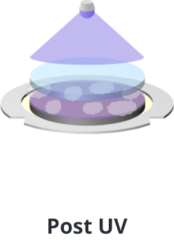
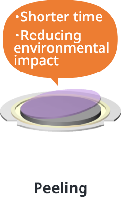
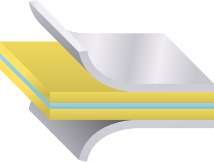
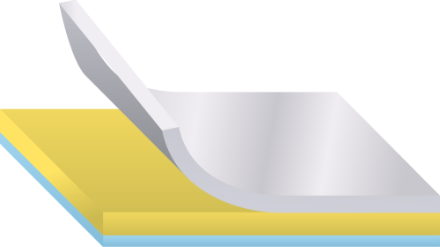
SELFA™'s Peeling-off Technology
SELFA™'s peeling-off demo video
You may find an advanced technology not found in other companies' products, enabling easy peeling-off without damaging the delicate wafer surface.
Two-step UV Irradiation
1Pre UV Curing
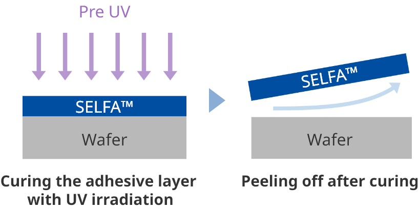
The adhesive strength of conventional UV tapes increases during thermal treatment and does not decrease significantly after UV exposure, making it difficult to be peeled off, leading to residue issues.
By curing the adhesive layer with Pre UV, SELFA™ significantly reduces adhesive strength which will not climb up sharply even after thermal treatment, making it much easier to be peeled off by much less force leaving much less residue.
2Gas Generation
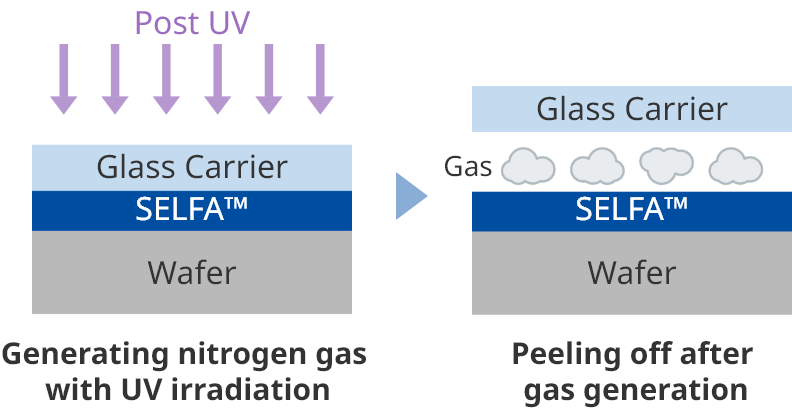
During the UV irradiation, nitrogen gas is generated between SELFA™ and the glass carrier. The gas region expands and eventually spreads across the entire surface.
After the UV irradiation, the carrier glass can be easily removed with almost no force.
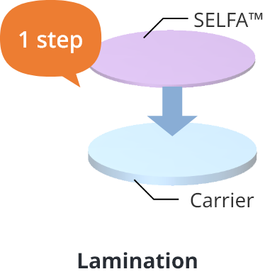
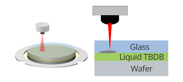
Comparison of Processes between SELFA™ and Liquid Materials
Using SELFA™ significantly shortens the Lamination and peeling processes.

Liquid
Materials
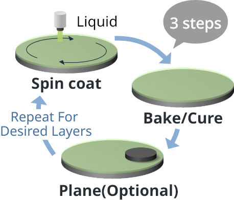
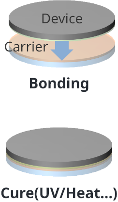
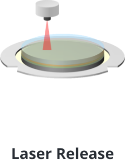
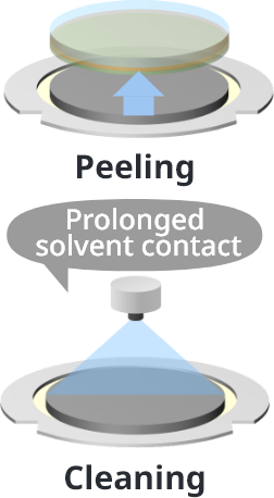
SELFA™
SEKISUIProduct Development Story
Continuing to support the evolution
of semiconductor processes with
innovative technology for
'adhesion and peeling'―
SELFA™
Former Director of the Research & Development Institute
(retired in 2019),
High Performance Plastics Company Current Representative of Science Lab Ishizue
Akira Nakasuga
Chief Engineer, Electronics Materials Development Center
Research & Development Institute
High Performance Plastics Company
Toshio Takahashi
SELFA™Lineup
Double Sided
Thermal Resistant
SELFA™ HW Series
BG ~ Dicing Process
- High resistance to heat and chemicals
- N2 Gas-release debonding mechanism results in damage free debonding
- Tape type adhesive supported glass carrier enables better
→handling capabilities
Single Sided Thermal Resistant SELFA™ HS Series
Device protection during chemical processesWarpage suppression during thermal processes

- High resistance to heat and chemicals
- High adhesion, low residue
Single Sided Self Release SELFA™ MP Series
Device protection during plating processes
- UV self-releasing function
→Easy peeling-off after the plating process
SELFA™ Structure and Properties
| Items and Conditions | HW Series | HS Series | MP Series | |
|---|---|---|---|---|
| Thermal Resistance | 260°C / Reflow | 250°C / Reflow | 80°C / 30min. | |
| 220°C / 2hr | 220°C / 2hr | |||
| Adhesion Strength (N/inch) Initial → Pre UV |
Wafer Side | SUS: 10.5 → 0.01 | SUS: 3.83 → 0.08 | SUS: 17.5 → 0 |
| Si: 0.08 → 0.02 | Si: 0.06 → 0.02 | Si: 16.1 → 0 | ||
| - | Cu: 4.51 → 0.10 | Au: 13.5 → 0 | ||
| Carrier Side | Glass: 0.06 → <0.01 | - | - | |
Application Examples
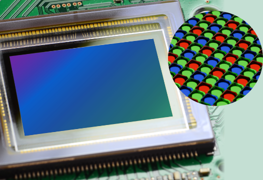
CMOS Image Sensor
- SELFA™ HW
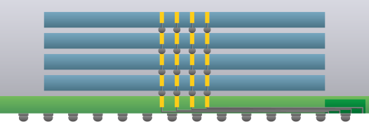
TSV
- SELFA™ HW
- SELFA™ HS

EMI
- SELFA™ HS
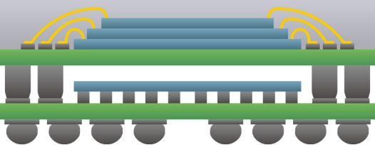
PoP
- SELFA™ HW
- SELFA™ HS
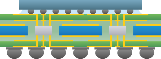
Fan Out / Embedded Substrate
- SELFA™ HW
- SELFA™ HS
- SELFA™ MP
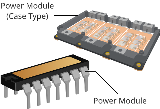
Power Device
- SELFA™ MP
Process Automation of Double-sided SELFA™
Compatible with fully automated processes, contributing to improve productivity and reduce environmental impact.
By partnering with equipment manufacturers, we can build fully automated equipment. Significant productivity improvements and reductions in environmental impact can be achieved.
Equipment Introduction
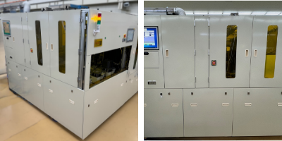
- ①Wafer Bonder
- Takatori Corporation
WSM-200B
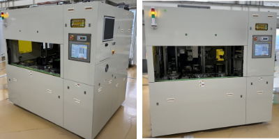
- ②Wafer Debonder
- Takatori Corporation
WSR-200
Reuse of Glass Carrier
By utilizing SELFA™, glass carriers can be reused more than twice much as before, also better for SDGs.
Carrier Glass Reusability
SELFA™ does not cause damage during UV irradiation, and is superior in terms of glass carriers’ recycling.
| SELFA™ | Liquid | |
| Times of reuse | Over 20 times | Over 10 times |
| Stripping method | UV Lamp UV Laser |
Various Lasers |
| Reuse methods | Solvent cleaning is the mainstream | Solvent cleaning, polishing, etc. |
| Glass damage | No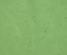 |
Yes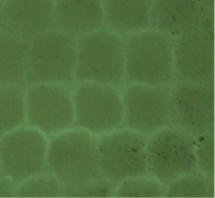 |
| Reason | 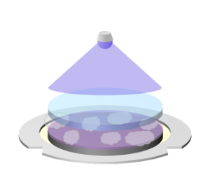 Significant less damage by UV lamp irradiation |
 More damage caused by laser ablation |
SEKISUIProduct Development Story
Continuing to support the evolution
of semiconductor processes with
innovative technology for
'adhesion and peeling'―
SELFA™
Former Director of the Research & Development Institute
(retired in 2019),
High Performance Plastics Company Current Representative of Science Lab Ishizue
Akira Nakasuga
Chief Engineer, Electronics Materials Development Center
Research & Development Institute
High Performance Plastics Company
Toshio Takahashi