Search by Device | Semiconductor- related
Production process flow related to semiconductors
The Electronics Strategy Office is running a wide material portfolio of tape/film/precise particles/sealing material. We are providing high functional products especially for the frontier needs in semiconductor industry, such as Fine L/S, high integrated design, 3D assembly, ultra thin membrane.
Wafer/chip production process
-

-

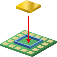
Protection Tape Lamination
High Adhesion-Easy Removable UV Tape Heat Resistant SELFA™ -

Back Grinding
-

Chemical Plating・High Temperture Treat
High Adhesion-Easy Removable UV Tape Heat Resistant SELFA™ -

Dicing Tape
Lamination -

UV Irradiation・Protection Tape Removing
-

-

Chip Completion
Package substrate production process
-

Copper Core Manufacture
-

Build Up Film
Build Up Film -

Via, Dismear, Plating,
Masking tape for semiconductor package substrates
Solder Resistant Coating. -

Print DAM material
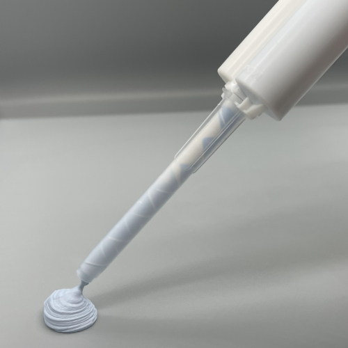
High-viscosity inkjet ink
Inkjet Material -

Package Substrate Completion
1+2Assembly production process


Tape
_ソルダーレジストマスキングテープ_png_w500px_h500px.png)
Solder Resist Making Tape
A thin-film masking tape that combines strong adhesion with easy peelability
_研磨布固定用両面テープ_ダブル_png_w500px_h500px.png)
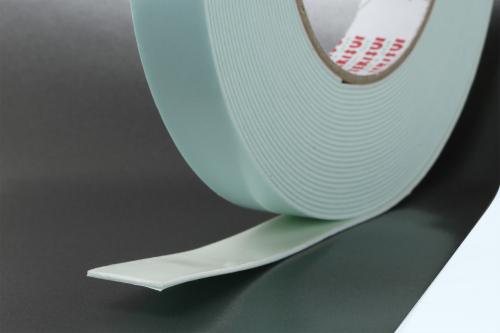
Double-sided Tape for Fixing Polishing Pads
A double-faced tape with a differential design that provides excellent adhesion and easy removability
/SELFA.png)
High-Heat-Resistance Temporary Fixing UV Tape SELFA™ Series
A high-heat-resistance, high-adhesion temporary fixing tape enabling easy removal through UV irradiation
Sheet
Film
_熱硬化型層間絶縁フィルム_png_w500px_h333px.png)
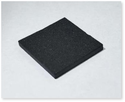
Foam
Adhesive
_インクジェット_png_w500px_h333px.png)
Microsphere・Filler
_ミクロパール™_png_w500px_h333px.png)
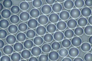
High-Performance Metal Plated Filler Micropearl™
High-performance functional filler that combines flexibility and conductivity without causing damage
Plastic-Based High-Performance Filler Micropearl™
High-performance fine particles that meet the needs of next-generation devices with precise thickness control and stress relaxation
_クリーン容器_png_w500px_h333px.png)