_熱硬化型層間絶縁フィルム_png_w500px_h333px.png)
_エレクトロニクス画像2_png_w500px_h333px.png)
Thermosetting Interlayer Insulating Film
Build-up film that contributes to finer wiring and high-speed communication in electronic devices.
- Electronics
- What is Build-up Film?
- Features
- Sekisui’s Strengths
- Current Product Lineup
- Applications
- Process Flow
- Contact Us
- Document download
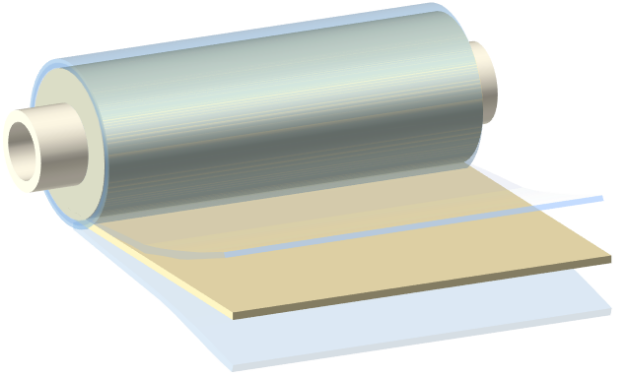
What is Build-up Film?
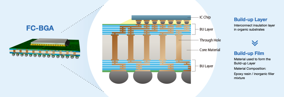
Build-up film is an interlayer dielectric material used to form fine wiring layers in advanced IC package substrates. As the performance of electronic devices improves, IC package substrates are also becoming denser to support higher speeds and improved performance. In addition to fine via formation capability and low dielectric properties, dimensional stability that suppresses warpage during processing and mounting has become increasingly important. These advanced IC package substrates are widely adopted in fields such as AI, servers, and network equipment. Build-up films have become essential materials that enable high-performance and high-reliability electronic devices.
Features
Sekisui Chemical’s build-up film combines excellent transmission characteristics and dimensional stability, with a proven track record in high-layer-count, large-size high-end IC package substrates (FC-BGA).
Its low dielectric and low-warping properties enhance design flexibility and contribute to the realization of next-generation devices with higher performance and reliability.
- Warpage
control - Low transmission loss
- FLS (Fine
Line Space) compatibility - Excellent embeddability
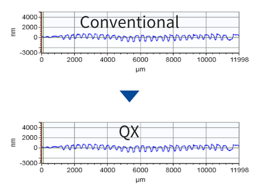
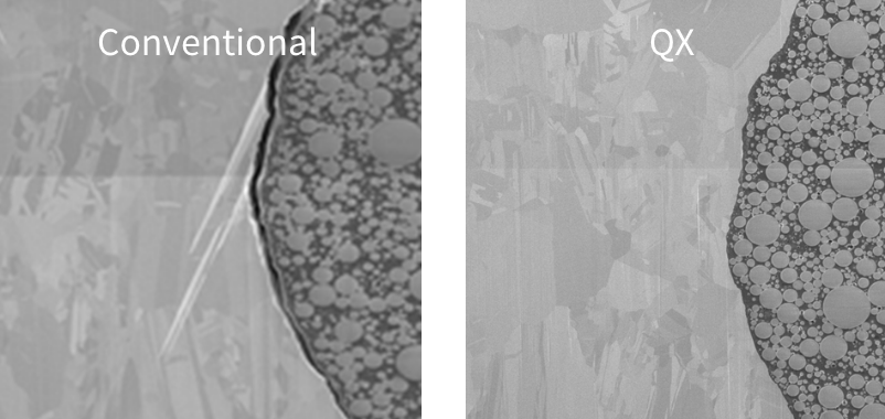
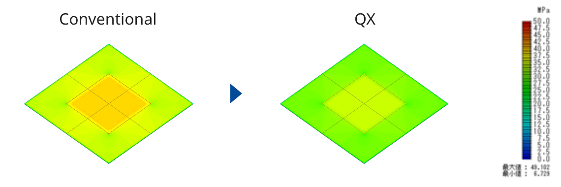
Sekisui’s Strengths
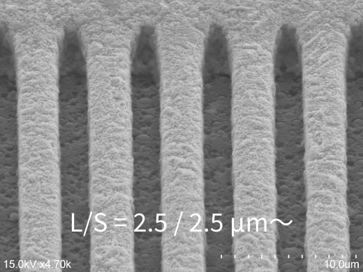
Sekisui Chemical’s build-up film achieves low dielectric loss (low Df), consistent surface roughness after desmear, and excellent crack resistance through proprietary compounding and coating technologies. These features contribute to low transmission loss, fine pattern compatibility, and improved yield required for next-generation package substrates.
Fine-pattern compatibility
BUF: QX / SEKISUI CHEMICAL Co., Ltd.
DFR: DA Series / Asahi Kasei Corp.
Exposure: DI Exposure / ADTEC Engineering Co., Ltd.
High embeddability & void suppression
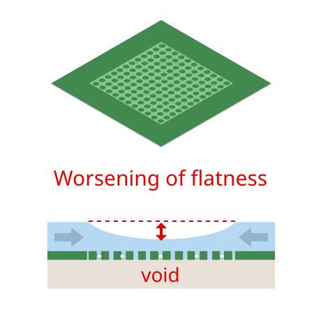
Low-stress design for delamination & warpage control
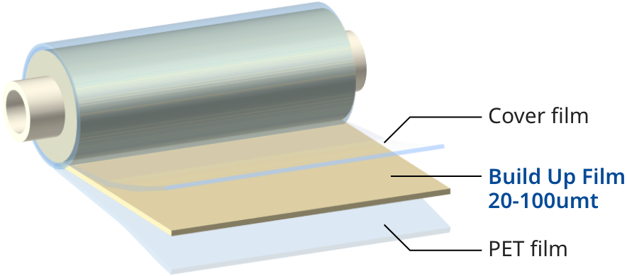
In addition, leveraging many years of tape manufacturing expertise, Sekisui can flexibly support various thickness requirements.
Standard products are available in 20–100 µm thickness (2.5 µm increments), and other thicknesses are available upon request.
Examples of SEKISUI Build-up Film Customers
(FC-BGA Manufacturers)
Current Product Lineup
| For FCBGA | For Embedded | ||||||
|---|---|---|---|---|---|---|---|
| NX04H | NQ07XP | QX03 | EL | TC | HE | ||
| HVM | Sampling | Development | Development | ||||
| Df | @5.8GHz | 0.0090 | 0.0037 | 0.0023 | ≦0.0025 | 0.0084 | 0.0050 |
| Dk | @5.8GHz | 3.3 | 3.3 | 3.3 | ≦2.5 | 3.4 | 5 |
| CTE (25-150℃) | ppm/℃ | 24.5 | 27 | 17 | 17-23 | 13 | 20 |
| Tg (DMA) | ℃ | 205 | 183 | 183 | > 170 | 206 | 170 |
| Young’s Modulus | GPa | 8 | 10.4 | 13.1 | > 7 | 12.3 | 20 |
| Elongation | % | 2.4 | 2.6 | 2.9 | > 1.5 | 1.2 | 1.2 |
| Tensile Strength | MPa | 100 | 105 | 110 | > 70 | 102 | 90 |
| Thermal Conductivity | W/m K | 0.5 | 0.5 | 0.6 | > 0.3 | 0.6 | 2.0 |
Applications
Sekisui Chemical’s build-up film is used in IC package substrates that perform advanced communication and computation processes, and is widely applied in the following fields.

 AI Processing Modules
- Offers thermal stability and process adaptability to meet the high heat generation and high-density wiring demands of GPUs and AI chips.
 Data Center Servers
- With excellent dielectric properties and durability, it contributes to the reliability of high-end server circuits that support large-scale data processing.
 Ethernet Switches
- Extensively adopted worldwide in high-speed network equipment that supports the 5G and cloud computing era.
 High-performance PCs & Workstations
- Balances signal integrity and manufacturing efficiency in increasingly complex, multilayered systems.
Process Flow
SEKISUI’s Build-up Dielectric Films are the ONLY alternative mass producing dielectric build-up material used in manufacturing of FC-BGA substrates with full compatibility with current Semi-Additive Process (SAP) manufacturing lines.
Several major substrate suppliers in Japan and Taiwan are manufacturing advanced FC-BGA substrates incorporating SEKISUI’s Build-up Dielectric Films and major OSATs have experience assembling those substrates.
Semi-Additive Process (SAP)
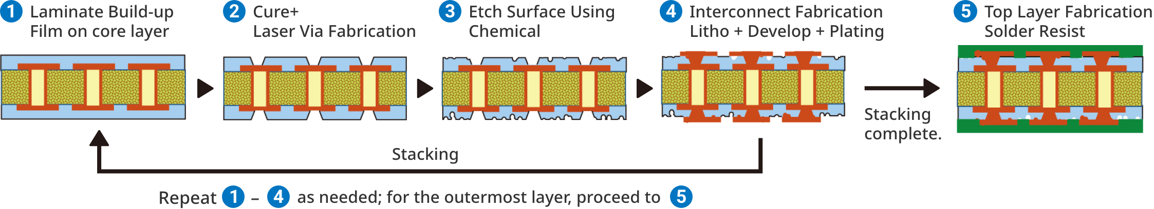
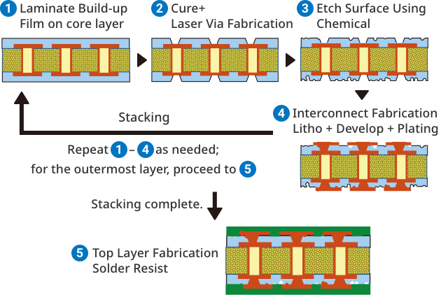
Please contact us if you need detailed SAP manufacturing conditions when using SEKISUI Build-up Dielectric Film
Contact Us
SEKISUI is continuously working with IC design houses, semiconductor manufacturers, and substrate suppliers to develop new build-up dielectric films to enable next generation challenges facing advanced substrates such as lowering Df to meet the needs of 224Gb Ethernet Switch Products and beyond.
Please contact us for any development needs.
- Looking to enhance the reliability of high-end server circuits
- Interested in developing a new build-up film etc.
Document download
- All
- Electronics
| Name | Type | File | Update | File |
|---|---|---|---|---|
| Catalog 〈Electronics〉:Thermosetting Interlayer Insulating Film | Electronics | 2025-09-30 | Download2.83 MB |