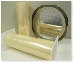
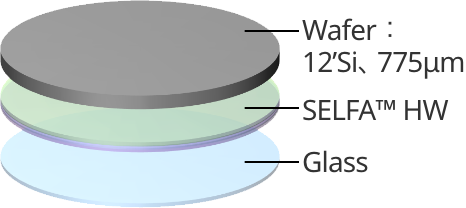
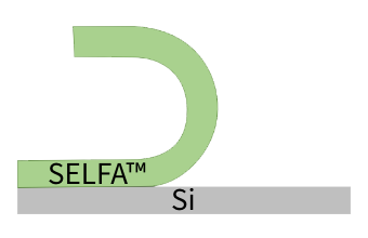
High-Heat-Resistance Temporary Fixing UV Tape SELFA™ Series
A high-heat-resistance, high-adhesion temporary fixing tape enabling easy removal through UV irradiation
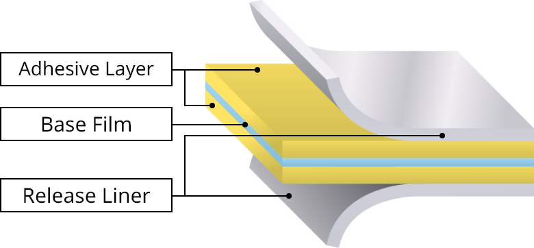
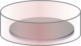
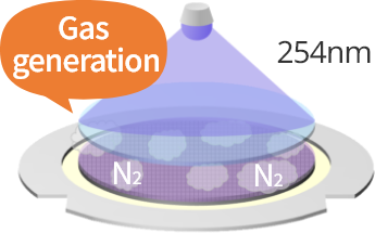
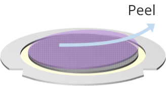
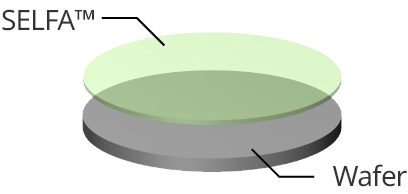
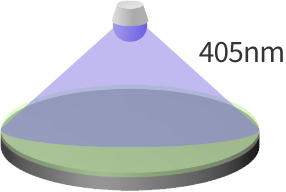
A UV release tape that combines strong adhesion with excellent peelability in semiconductor wafer and chip processing. They utilize proprietary technology to generate gas under UV irradiation, enabling clean removal without causing wafer damage. With excellent heat and chemical resistance, the lineup is suitable for diverse manufacturing processes.
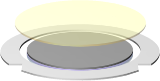
Using tape type adhesive to support glass carrier enables better handling capabilities. N2 Gas-release debonding mechanism results in damage free debonding. High resistance to heat and chemicals.
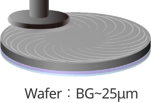
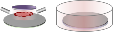
Process
Laminating
Bonding
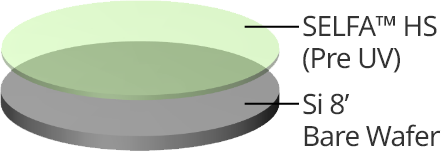
Pre UV
BG
Thermal Process
Dicing Tape
Post UV & DB
De-Taping
Evaluation results
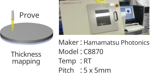
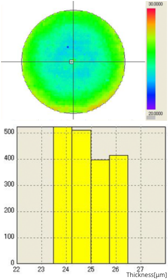
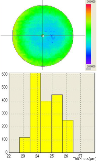
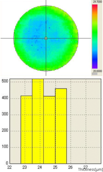
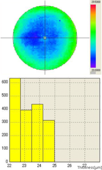
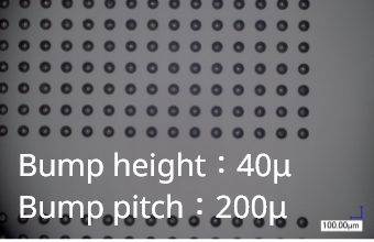
Ⅰ.Mirror Wafer TTV Evaluation after BG
Evaluation Method
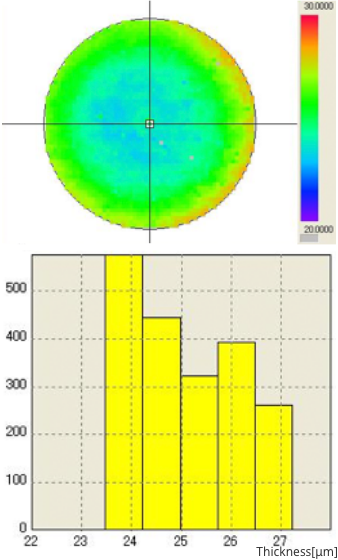
TTV Mapping Result
【Average】 Thickness : 24.4μm/ TTV : 2.9μm
n=1
n=2
n=3
n=4
n=5
Thk:25.1μm TTV:3.4μm
Thk:24.5μm TTV:2.8μm
Thk:24.7μm TTV:2.9μm
Thk:24.3μm TTV:2.7μm
Thk:23.4μm TTV:2.9μm
Our unique “PreUV technology” can provide industry’s highest level TTV controllability.
<3μm@12” wafer
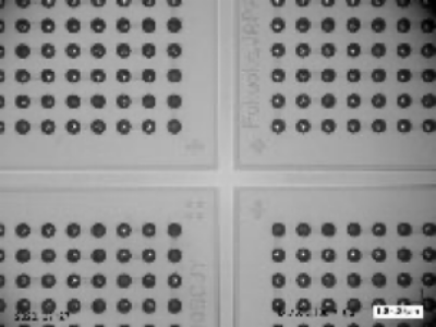
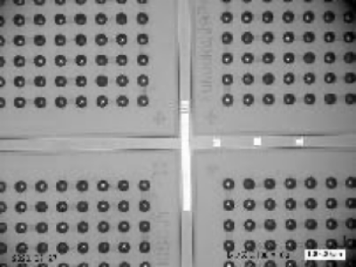
Ⅱ.Residue After Thermal Process<Oven and De-taping evaluation>
Point :
Thermal resistant
Equipment & Conditions
Maker: ETAC
Model: CSO-603BF
Temp: 180〜220°C
Time: 1〜2hr
Wafer & Sample
8inch Bump TEG Wafer
Results
180°C
200°C
220°C
1hr
2hr
No residue on the patterned TEG wafer after a thermal stress of 220°C 2hr.
Single Sided Thermal Resistant SELFA™ HS Series
Characteristic:
Thermal Resistance
Chemical Resistance
Low Residue
Supports and protects devices during thermal processes such as reflow, CVD, and sputtering.
Process
Laminating
Pre UV
BG
Transporting
Thermal Processes
De-Taping
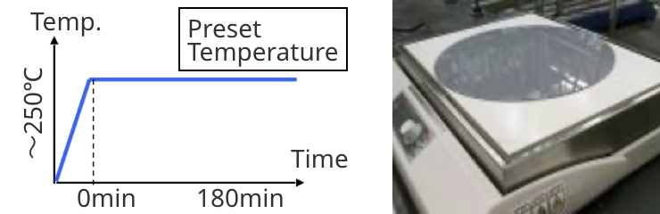
Thermal Resistance Evaluation (Void)
Hot Plate Evaluation
Sample
Equipment & Conditions
Maker: NINOS
Model: ND-3H
Temp: 180-250°C
Time: 30-180min
Results
Peeling-off Ability After Heating
30min
60min
120min
180min
180°C
OK
OK
OK
OK
220°C
OK
OK
OK
OK
250°C
OK
OK
OK
OK
The data shown above is measurement value, not guaranteed value.
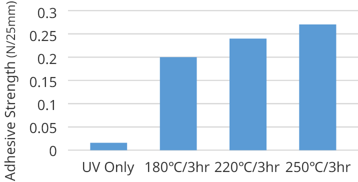
Adhesive Strength After Heating
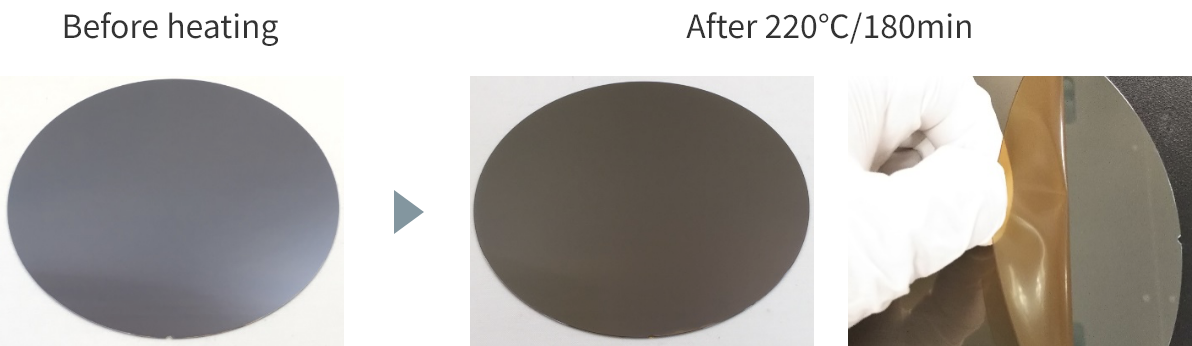
Wafer State After Heating
In hot plate evaluations, it has been confirmed that no void occurs during thermal treatment and no residue is generated during peeling, even at up to 220°C for 180 minutes.
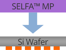
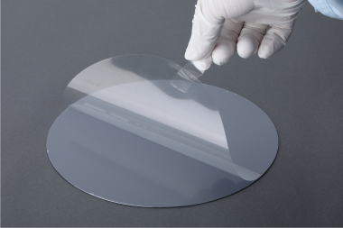
Single sided Self Release SELFA™ MP Series
Characteristic:
Easy-peeling
SELFA™ MP is used for protecting the backside of wafers during plating processes. UV irradiation generates gas, allowing it to be peeled off from the subject easily.
The Wafer Protection Process During Electroless Plating Treatment (Electroless Plating Method)
Tape lamination
Acid, alkali plating process
UV irradiation
After de-taping
SELFA™ MP has excellent resistance to strong acids and strong alkalis during the plating process, and after protecting the wafer, it can be peeled off with low stress.
Voids and Residue Results
Point:
Easy-peeling
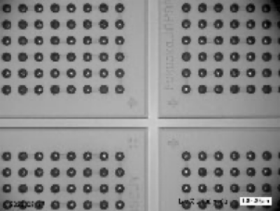
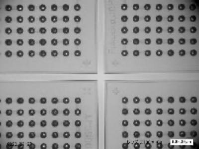
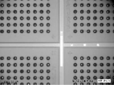
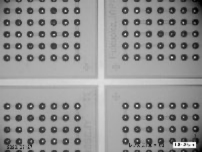
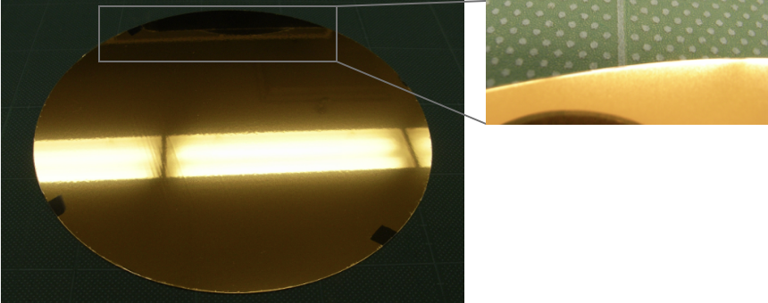
Wafer After Au Plating
No void, no edge delamination
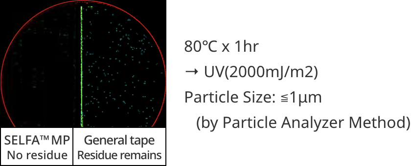
Organic Residue Inspection @8’ Wafer
No residue was observed after peeling off SELFA™ MP
Document download
All
Electronics
Name
Type
File
Update
File
Catalog 〈Electronics〉:High-Heat-Resistance Temporary Fixing UV Tape SELFA™ Series
/SELFA.png)
/SELFA剥がし方.png)